Large-area Epitaxial Growth of van der Waals (vdW) Materials
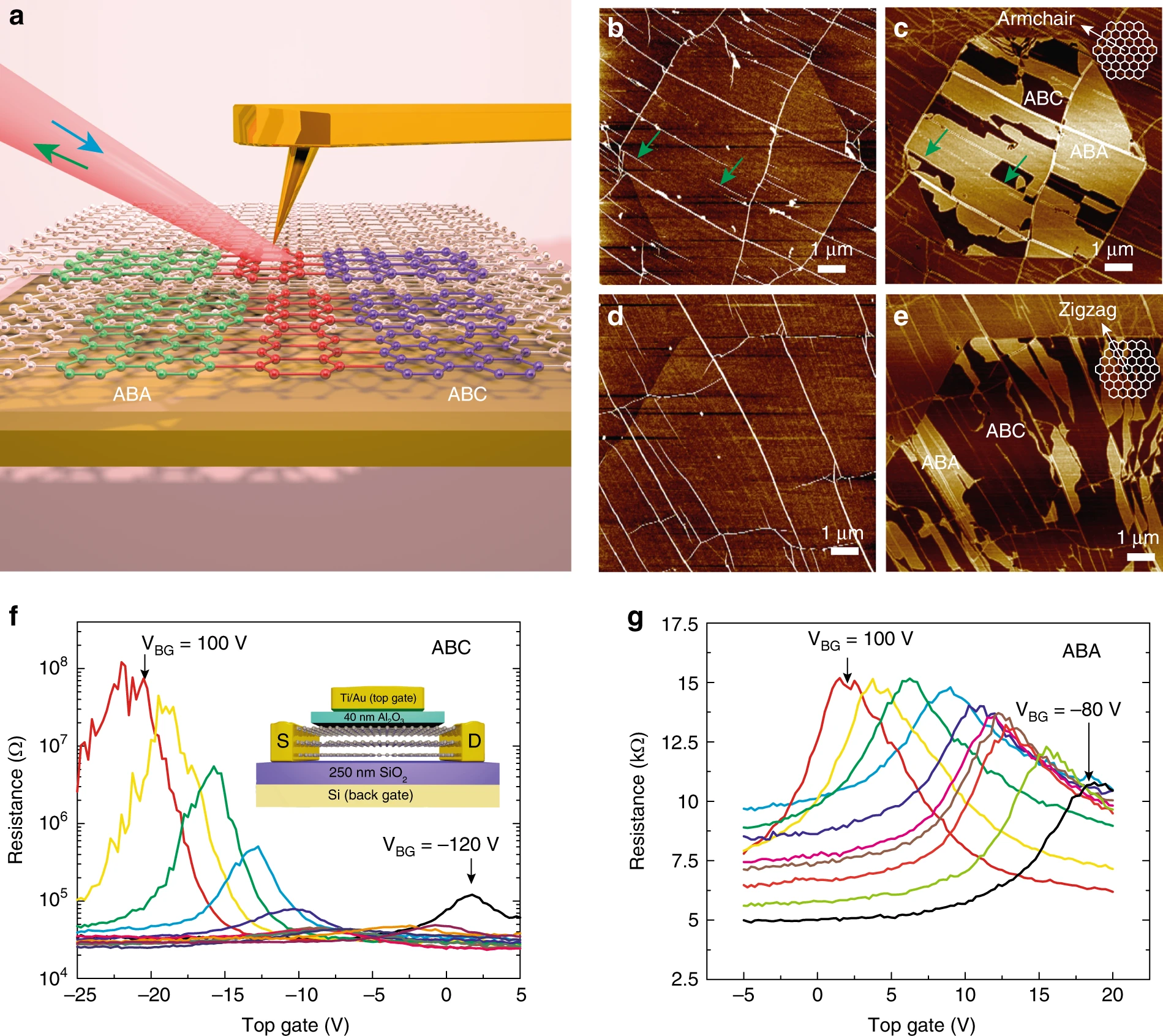
The properties of van der Waals (vdW) materials often vary dramatically with the atomic stacking order between layers, but this order can be difficult to control. Trilayer graphene (TLG) stacks in either a semimetallic ABA or a semiconducting ABC configuration with a gate-tunable band gap, but the latter has only been produced by exfoliation. We presented a chemical vapor deposition approach to TLG growth that yields greatly enhanced fraction and size of ABC domains. The key insight is that substrate curvature can stabilize ABC domains. Controllable ABC yields ~59% were achieved by tailoring substrate curvature levels. ABC fractions remained high after transfer to device substrates, as confirmed by transport measurements revealing the expected tunable ABC band gap. Substrate topography engineering provides a path to large-scale synthesis of epitaxial ABC-TLG and other vdW materials.
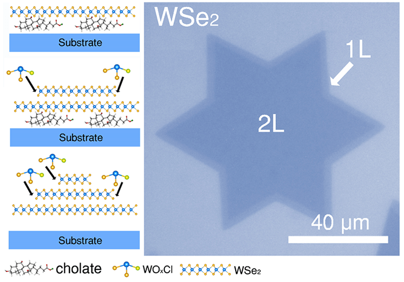
Bilayer two-dimensional (2D) van der Waals (vdW) materials are attracting increasing attention due to their predicted high quality electronic and optical properties. We demonstrated dense, selective growth of WSe2 bilayer flakes by chemical vapor deposition with the use of a 1:10 molar mixture of sodium cholate and sodium chloride as the growth promoter to control the local diffusion of W-containing species. A large fraction of the bilayer WSe2 flakes showed a 0 (AB) and 60° (AA′) twist between the two layers, whereas Moiré 15 and 30° twist angles were also observed. Well-defined monolayer−bilayer junctions were formed in the as-grown bilayer WSe2 flakes, and these interfaces exhibited p−n diode rectification and an ambipolar transport characteristic. This work provides an efficient method for the layer-controlled growth of 2D materials, in particular, 2D transition metal dichalcogenides, and promotes their applications in next-generation electronic and optoelectronic devices.
Graphene Field-Effect Biosensors Arrays
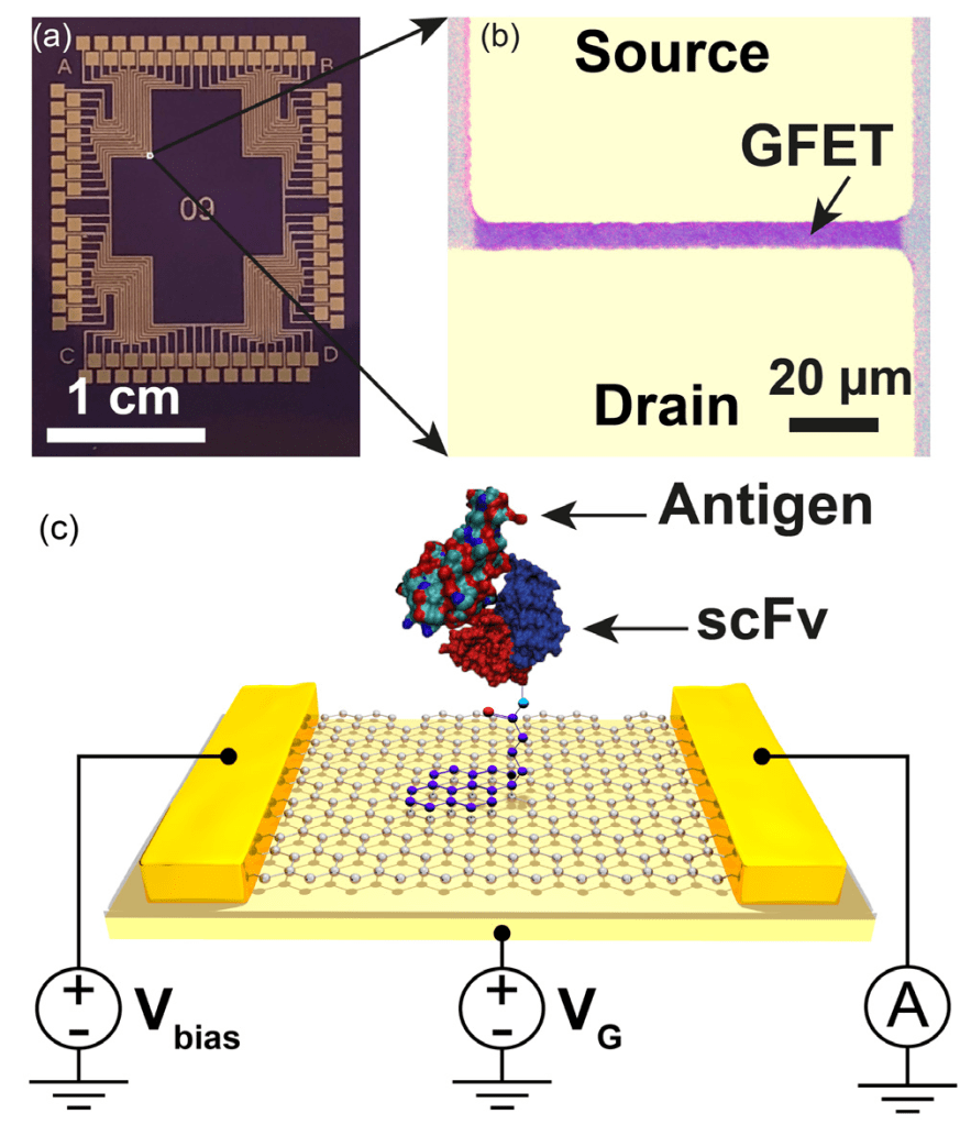
Lyme disease is an infectious disease caused by the Borrelia burgdorferi bacterium. Early diagnosis of Lyme disease could prevent patients from developing serious side effects such as chronic arthritis and permanent neurological disorders. Lyme disease diagnosis is currently held back by a lack of reliable tools that are sufficiently sensitive and specific to allow early stage detection. Here, we demonstrate all electronic nano-biosensors for multiplexed detection of antigens of B. burgdorferi at concentrations as low as 2 pg ml−1. The sensors are based on graphene field-effect transistors (GFETs) coupled with genetically engineered antibody fragments. Single-chain variable fragment (scFv) antibodies are used to obtain a closer proximity of the target-binding event to the graphene sensor surface and for higher immobilization density. When compared to GFET nano-biosensors that use the parental immunoglobulin G (IgG) antibodies, scFv GFET nano-biosensors achieve approximately a 4000 × improvement to the limit of detection. We also demonstrate multiplexed detection of B. burgdorferi antigens through site-specific immobilization of scFvs on GFET arrays, which can potentially reduce the false-positive diagnosis ratio of Lyme disease. This work offers a pathway towards point-of-care detection of Lyme disease at an early stage.
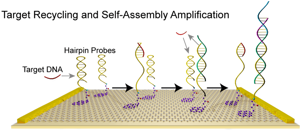
All-electronic DNA biosensors based on graphene field-effect transistors (GFETs) offer the prospect of simple and cost-effective diagnostics. For GFET sensors based on complementary probe DNA, the sensitivity is limited by the binding affinity of the target oligonucleotide, in the nM range for 20 mer targets. We report a ∼20 000× improvement in sensitivity through the use of engineered hairpin probe DNA that allows for target recycling and hybridization chain reaction. This enables detection of 21 mer target DNA at sub-fM concentration and provides superior specificity against single-base mismatched oligomers. The work is based on a scalable fabrication process for biosensor arrays that is suitable for multiplexed detection. This approach overcomes the binding affinity- dependent sensitivity of nucleic acid biosensors and offers a pathway toward multiplexed and label-free nucleic acid testing with high accuracy and selectivity.
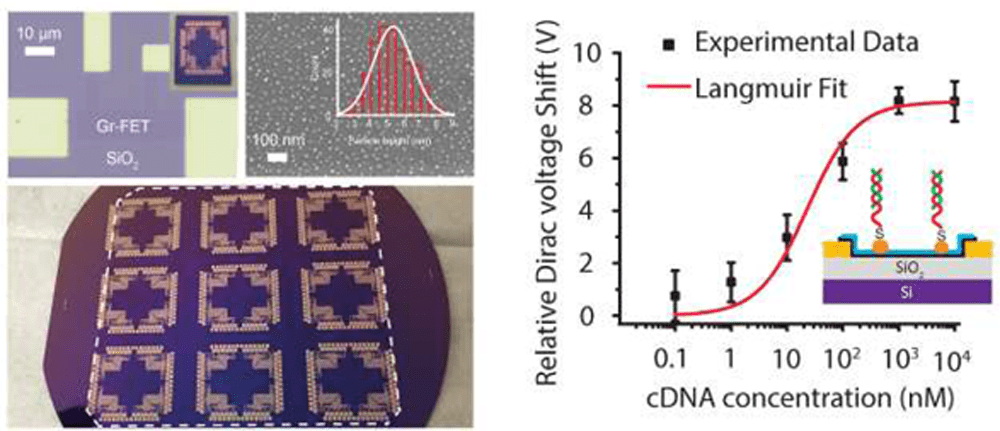
We have developed a scalable fabrication process for the production of DNA biosensors based on gold nanoparticle-decorated graphene field effect transistors (AuNP-Gr-FETs), where monodisperse AuNPs are created through physical vapor deposition followed by thermal annealing. The FETs are created in a four-probe configuration, using an optimized bilayer photolithography process that yields chemically clean devices, as confirmed by XPS and AFM, with high carrier mobility (3590 ± 710 cm2/V·s) and low unintended doping (Dirac voltages of 9.4 ± 2.7 V). The AuNP-Gr-FETs were readily functionalized with thiolated probe DNA to yield DNA biosensors with a detection limit of 1 nM and high specificity against noncomplementary DNA. Our work provides a pathway toward the scalable fabrication of high-performance AuNP-Gr-FET devices for label-free nucleic acid testing in a realistic clinical setting.
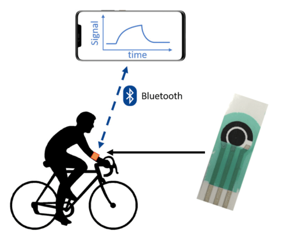
Wearable Sensors for Real-time Analysis of Human Sweat
Wearable sweat biosensors are emerging as a powerful tool to monitor the health status and sports performance of an individual in a non-invasive way. The key biomarkers in human sweat, such as electrolytes, metabolites, and hormones, are correlated with their concentrations in blood and reflect one’s stress level, hydration status, and physiological state. The development of wearable devices that can detect these biomarkers with high accuracy and selectivity holds tremendous promise for commercial applications, such as health and wellness, sports, baby monitoring, elderly care, early-stage disease diagnosis, and more. With the ability to continuously monitor an individual’s physiological status, the as-proposed wearable sweat sensor would thus offer a wide range of applications in medical healthcare and sports science.